Here's what we know about Nvidia Ampere GPUs after Jen-Hsun's keynote
Apart from the fact that our Nvidia's leather jacket wearing CEO has a serious thing for spatulas...

That's it, the Nvidia Ampere GTC Keynoteis over. Jensen Huang was back in his trademark black leather jacket, and all was instantly right with the world. We all got to see inside the Nvidia CEO's kitchen, and marvel at the number of spatulas he has (honestly, why so many spatulas?).
Kitchen paraphernalia aside, the keynote was made up of eight videos, covering everything from autonomous driving, medical research, conversational AI, and robotics—which are all important for Nvidia, but not us gamers. After all of that you may be left thinking that there was no real information about Nvidia's next gaming graphics cards. And while there were a few mentions of gaming graphics, there were no direct details about the hardware itself.
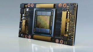
What the GTC keynote did have though, was a whole lot of details on the A100. While the A100 is designed for data centres, the same architecture will make it's way into next-gen GeForce graphics cards some time in the future.
| Header Cell - Column 0 | Peak Performance |
|---|---|
| Transistor Count | 54 billion |
| Die Size | 826mm² |
| FP64 CUDA Cores | 3,456 |
| FP32 CUDA Cores | 6,912 |
| Tensor Cores | 432 |
| Streaming Multiprocessors | 108 |
| GPU Memory | 40GB |
| GPU Memory Bandwidth | 1.6 TB/s |
| Interconenct | NVLink 600 GB/s | PCIe Gen 4 64GB/s |
| Multi-Instance GPUs | Various Instance sizes with up to 7MIGs @ 5GB |
| Form Factor | 4 / 8 SXM GPUs in HGX A100 |
| Max Power | 400W (SXM) |
The big take away about the A100 is that it is a big chip, and I'm not just talking about its physical size, although at 826mm square it's beefy, it's more the fact that it has squeezed 54 billion transistors in there. It's not easy to make direct comparisons with the current Turing architecture here, as Nvidia's previous data center offering was the Volta V100, but still there are some serious step ups in terms of performance. Nvidia claims a 20x performance increase over Volta in certain tasks. For comparison that chip had 21.1bn transistors and measured 815mm square. So the A100 has 2.5x the transistors, but is only slightly bigger. That's the jump to TSMC's 7nm process showing its worth.

If you're looking for some real time ray tracing, then the second video has plenty of footage of Minecraft RTX, and a delightful marble game called… Marble RTX. There was no talk about ray tracing RT Cores though, as they're not used in data centers, but Tensor Core performance does appear to have increased considerably. (Although they've changed, so there isn't an easy comparison here).
The actual number of tensor cores per SM has dropped to four (Turing had eight), but Nvidia still claims an overall performance increase—in some scenarios as much as 2.5x. Those rumours that the tensor performance was going to increase appear to be on the money, we just hadn't expected there to actually be less cores overall.
What we don't know from all of this is what sort of performance we'll be getting in the next-generation graphics cards. We don't have the core counts, the clock speeds, or anything like that at this stage, although be sure to check out the everything we know about Nvidia Ampere for the latest info.
The biggest gaming news, reviews and hardware deals
Keep up to date with the most important stories and the best deals, as picked by the PC Gamer team.
Alan has been writing about PC tech since before 3D graphics cards existed, and still vividly recalls having to fight with MS-DOS just to get games to load. He fondly remembers the killer combo of a Matrox Millenium and 3dfx Voodoo, and seeing Lara Croft in 3D for the first time. He's very glad hardware has advanced as much as it has though, and is particularly happy when putting the latest M.2 NVMe SSDs, AMD processors, and laptops through their paces. He has a long-lasting Magic: The Gathering obsession but limits this to MTG Arena these days.
Most Popular


