Asus China's general manager shows off the deep details of Intel's Arrow Lake chips in new reveal
There can't be many top managers as cool as Ordinary Uncle Tony.

We're just a week or so away from the retail launch of Intel's Arrow Lake chips and while Team Blue has already given us the full lowdown of what everything is like, there's nothing cooler than seeing the actual chips in their full glory. Enter stage left, Tony Yu, Asus China's general manager, and his Bilibili channel, Ordinary Uncle Tony, to sate that interest.
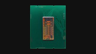
I spotted Tony Yu's Bilibili video thanks to Uniko's Hardware on X and it's a real treat for processor enthusiasts. We're big fans of Fritzchen Fritz here, who takes some of the most incredible images of chip dies you've ever seen, but Yu's video goes one step further by explaining all of the key parts in each tile in the new Arrow Lake CPUs.
As you're probably already aware, rather than using a single slab of silicon for the whole processor (known as a monolithic design), Arrow Lake follows on from Meteor Lake by using several slices (aka tiles or chiplets) that are all mounted on a separate die, so it can be packaged as a single chip.
Every Arrow Lake processor comprises a compute tile (home to the P- and E-cores, and L3 cache), a SoC tile (housing the neural processor, media engine, DDR5 memory controller, and PCIe controller), an IO tile to handle all the data connections, and teeny tiny GPU tile. Oh, and two blank tiles to fill up the empty spaces.
Altogether, these tiles make a single processor that's a little larger than a Raptor Lake die but because they're manufactured on different TSMC process nodes, certain costs can be reduced. For example, the IO and SoC tiles are made on the relatively old and cheap N6 node, whereas the compute tile uses the latest N3B one.


That particular tile is the most noteworthy as it contains the new P- and E-cores, codenamed Lion Cove and Skymont respectively. These are markedly better than those in Raptor Lake, according to Intel, and you can easily see that the layout is quite different too. Rather than having two massive blocks of different cores, Arrow Lake now has them somewhat dispersed to help prevent hotspots.
While Arrow Lake chips still top out at 36 MB of L3 cache like Raptor Lake, the P-cores now have 3 MB of L2 cache compared to 2 MB previously. The E-cores don't get any more L2 cache but they're massively better than the old E-cores, as we've already seen in Lunar Lake.
The biggest gaming news, reviews and hardware deals
Keep up to date with the most important stories and the best deals, as picked by the PC Gamer team.
Images like these remind me just how astonishingly complex modern processors are and it's somewhat of a minor miracle that, for the most part, you can just drop one into a motherboard, connect a few wires, load some software, and it all just works.
Now, as to how well Arrow Lake works in the real world, we don't have too long to wait. Reviews and retail availability all launch on 24 October, so it's just a few days really before you'll know if Arrow Lake is worth upgrading to.
Until then, just sit back and stare at the beauty of what Intel has created. No matter how good or bad it turns out to be, you can't deny that it's a glorious thing to look at.
Best CPU for gaming: Top chips from Intel and AMD.
Best gaming motherboard: The right boards.
Best graphics card: Your perfect pixel-pusher awaits.
Best SSD for gaming: Get into the game first.

Nick, gaming, and computers all first met in 1981, with the love affair starting on a Sinclair ZX81 in kit form and a book on ZX Basic. He ended up becoming a physics and IT teacher, but by the late 1990s decided it was time to cut his teeth writing for a long defunct UK tech site. He went on to do the same at Madonion, helping to write the help files for 3DMark and PCMark. After a short stint working at Beyond3D.com, Nick joined Futuremark (MadOnion rebranded) full-time, as editor-in-chief for its gaming and hardware section, YouGamers. After the site shutdown, he became an engineering and computing lecturer for many years, but missed the writing bug. Cue four years at TechSpot.com and over 100 long articles on anything and everything. He freely admits to being far too obsessed with GPUs and open world grindy RPGs, but who isn't these days?

Nvidia has reportedly killed production of all RTX 40 GPUs apart from the 4050 and 4060 as affordable 50-series GPUs could arrive earlier than expected

AMD's 2025 laptop plans sure do include a lot of refreshed and rebranded APUs, but who cares when you've got Fire Range, Strix Halo, and four RDNA 4 mobile GPUs heading our way next year
Most Popular


