PlayStation 5 Pro hardware leak suggests its GPU is a RDNA 3/4-hybrid design, with some big improvements coming this way
I'll stick be sticking with my gaming PC, of course.

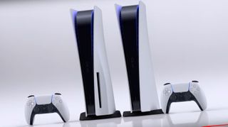
Hot on the tails of the rumour that Sony is planning on releasing its own upscaling technology, with the forthcoming PlayStation 5 Pro, comes a wealth of tidbits purporting to be what the next-gen console's hardware is going to be like. The CPU will still be the same ol' Zen 2 core, and the RAM's a bit faster, but the GPU is getting replaced with a whole new design. And it's seemingly a funky blend of RDNA 3 and RDNA 4.
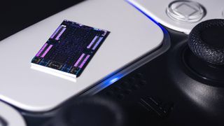
The leaks in question come from Inside Gaming and while they are unsubstantiated claims, the details seem credible enough to me. For example, it's being said that the PS5 Pro's custom AMD APU retains the same Zen 2-powered CPU as in the original PlayStation 5. So that's still eight cores and 16 threads, but that's fine for the majority of games.
It won't be running any faster, though apparently there will be an additional operating mode, letting it draw more power to achieve a 10% higher clock speed. That will come at a cost to the GPU, which would receive less power in that mode, though only losing around 1% of its performance. Why wouldn't Sony go with a faster CPU? The answer to that is simple: Backwards compatibility. All PS5 games, and older ones that also run on the platform, expect a CPU running at 3.5 GHz at best. Changing that by too much could mess up a lot of things.
The same is true of the system RAM. There's 16GB of average speed GDDR6 inside every PS5, and access to it is shared by the CPU and GPU. Running at 14 Gbps on a 256-bit aggregated memory bus, there's a fairly measly 448 GB/s of total bandwidth on offer. The PS5 Pro will apparently offer 576 GB/s of bandwidth and assuming the bus width has changed, that equates to a speed of 18 Gbps.
To put those figures into perspective, the Radeon RX 6800 and RX 7800 XT both have 256-bit buses, but the former uses 16 Gbps GDDR6, whereas the latter has chips running at 19.5 Gbps for 624 GB/s of bandwidth. On paper, that would make the PS5 Pro look especially nice, as the RX 7800 XT is no slouch, but that GPU also packs 64 MB of Level 3 cache (aka Infinity Cache) to reduce the load on the VRAM.

There's no sign of the PS5 Pro's APU getting Infinity Cache, because AMD and Sony need the chip to be as small as possible, in order to keep manufacturing costs down. But since the CPU and GPU are using the same pool of RAM, that 576 GB/s of bandwidth is going to be hit hard. Especially when you read about the claimed changes to the graphics processor.
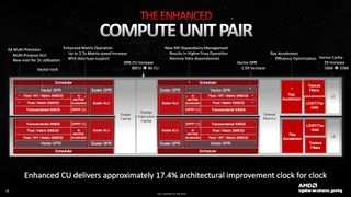
In the original PS5, the GPU is almost like an RDNA 2 processor, with 36 Compute Units (CUs) paired into 18 Workgroup Processors (WGPs). Inside each CU are two banks of 32 ALUs, that handle all of the shaders. The rumours for the PS5 Pro claim that the new GPU sports 30 WGPs, the same as the RX 7800 XT, for a peak FP32 throughput of 33.5 TFLOPS.
The biggest gaming news, reviews and hardware deals
Keep up to date with the most important stories and the best deals, as picked by the PC Gamer team.
If both of those figures are correct, then the only way this could happen is if the CUs are based on the RDNA 3 architecture, which means they have two banks of 64 ALUs. A quick calculation on a bit of paper puts the boost clock at 2,180 MHz, which is lower than the PS5's but the extra shaders more than make up for it.
However, we're also being told the Ray Accelerators in the CUs support BVH8 traversal shaders. BVHs, or bounding volume hierarchies, are data structures used to speed up working out which object a light ray is interacting with and in RDNA 3, the shaders work on four BVH children from each node (aka BVH4).

Increasing this to eight means, in theory, that the PS5 Pro GPU should be able to work through the traversal process a lot quicker than previously. Potentially, at least, as it's not as simple as 'the number is doubled and so is the performance'. While there's no indication that AMD has shifted these operations off the CUs and onto dedicated hardware units (like Nvidia does with its GPUs), the change in the traversal shaders tells us that the new GPU is not a pure RDNA 3 one but instead an RDNA 3/4 hybrid.
It's unlikely to be a total RDNA 4 design because of it not having any Infinity Cache, but if the figures are all to be believed, it's more RDNA 4 than 3. The key sign for this is claim over the AI Accelerators, which first appeared in RDNA 3. In the PS5 Pro's chip, they are purported to reach 300 TOPS in INT8 mode and 67 TFLOPS in FP16 mode.
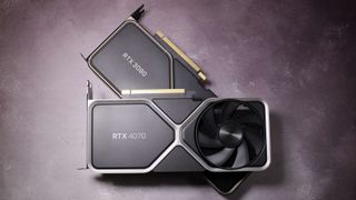
The RDNA 3-powered Radeon RX 7800 XT, for example, can do 512 INT8/FP16 operations per CU per clock cycle, on its AI accelerators, which means peaks of 75 TOPS and 75 TFLOPS respectively. For comparison, the Tensor cores in Nvidia's GeForce RTX 3090 Ti have a peak INT8 throughput of 320 TOPS.
What use would all that be for? AI, be it in the form of upscaling or any other task that machine learning can be applied to.

Best CPU for gaming: The top chips from Intel and AMD.
Best gaming motherboard: The right boards.
Best graphics card: Your perfect pixel-pusher awaits.
Best SSD for gaming: Get into the game ahead of the rest.
At this stage, it's all ifs and buts, and there's no guarantee whatsoever that any of this is true. But machine learning and ray tracing performance have previously been RDNA's Achilles' heel, so it makes a lot of sense that AMD would significantly improve them for RDNA 4, given how important machine learning workloads are these days.
I'm unlikely to go out and buy a PlayStation 5 Pro when it launches, given that there's a perfectly decent PS5 already in use in my house and a multitude of gaming PCs, but from a tech writer's perspective, it looks quite promising.
From a GPU enthusiast point of view, though, RDNA 4 is looking mightily interesting: It may not end up right at the top of the performance charts, but it looks like it will have all the features you could want.

Nick, gaming, and computers all first met in 1981, with the love affair starting on a Sinclair ZX81 in kit form and a book on ZX Basic. He ended up becoming a physics and IT teacher, but by the late 1990s decided it was time to cut his teeth writing for a long defunct UK tech site. He went on to do the same at Madonion, helping to write the help files for 3DMark and PCMark. After a short stint working at Beyond3D.com, Nick joined Futuremark (MadOnion rebranded) full-time, as editor-in-chief for its gaming and hardware section, YouGamers. After the site shutdown, he became an engineering and computing lecturer for many years, but missed the writing bug. Cue four years at TechSpot.com and over 100 long articles on anything and everything. He freely admits to being far too obsessed with GPUs and open world grindy RPGs, but who isn't these days?
Most Popular


